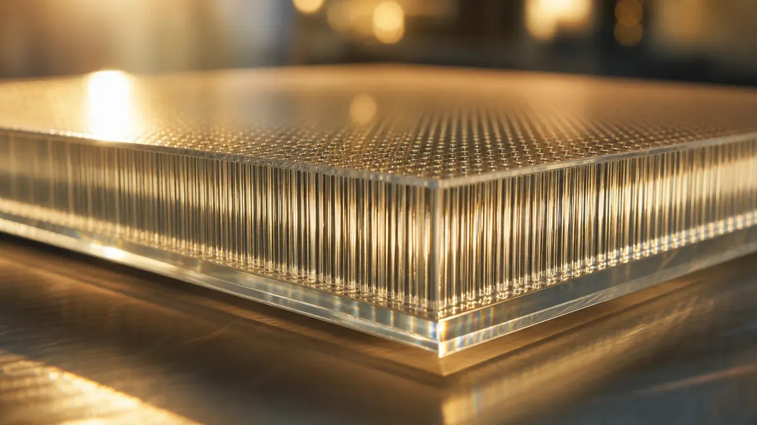
The advanced-packaging gate explained that, as transistors get harder to shrink, the industry has shifted to finding performance in “how you assemble the chips together.” But however much the assembly methods improve, the “board that carries the chip” underneath them has to keep up too. AI chips keep getting bigger and more power-hungry, today’s organic carrier boards are starting to buckle, and so the industry is turning to a material that’s older yet steadier: glass.
This piece spells out the glass substrate. First what it is and how it differs from today’s carrier, then its advantages and hurdles, the critical TGV process, and finally a sweep of where the international players and Taiwan players each stand. Let’s put the conclusion up front: its prospects draw plenty of hope, but 2026 is still a “pilot year,” and “volume” is still some distance off. This is the extended materials chapter of The AI Hardware Supply Chain, End to End.
What Is a Glass Substrate?
To understand the glass substrate, first look at what the “carrier board” inside a package does. The carrier (substrate) is the layer sandwiched between the chip and the motherboard; it holds the chip and routes its densely packed wiring out. The carrier in today’s high-end chips has a core made of an organic resin called ABF (an organic insulating material commonly used in high-end packaging carriers).
A glass substrate, as the name suggests, swaps the “core layer” of that carrier from organic resin to glass. Note that this isn’t as simple as “glass fully replaces ABF.” A more precise way to put it: an organic core layer is replaced with a glass core layer, while the outer layers still typically pair with redistribution, copper interconnect, and other structures. In other words, glass replaces the foundation deepest inside — it doesn’t tear down and rebuild the whole building.
An analogy: if an organic carrier is like a wooden board that warps slightly when it takes on moisture, a glass substrate is like swapping in a flat, hard glass board that isn’t too afraid of heat — and the higher and larger you build, the more the steadiness of that foundation matters.
Core-Data Snapshot
A few numbers to help you grasp where the glass substrate stands now. A reminder: most of these are each company’s “targets” or research-firm estimates, and the timing is still subject to change.
| Topic | Data | Timing / Nature |
|---|---|---|
| Overall mass-production timeline | Most makers target small volumes from 2027 and large-scale adoption in 2028-2030 | Company targets / research-firm estimates, timing varies |
| Intel glass substrate | Has built a working test vehicle; officially uncommitted on a mass-production timeline (placed at the tail end of a decade-long roadmap) | Intel official white paper |
| Via-density advantage | Glass TGV pitch around 100µm, versus around 325µm for an organic carrier — up to roughly 10× the density | Intel official figures |
| Absolics (SKC) | Georgia plant received CHIPS funding of up to US$75 million; capacity estimated to start in 2027 | US NIST announcement |
| Samsung Electro-Mechanics (SEMCO) | Sejong pilot line, pilot production in 2026, targeting mass production around 2027 | Samsung official / Korean media |
| Taiwan players’ stage | Innolux, AUO, Unimicron, and others are mostly in R&D, sample validation, or pilot production — not yet mass production | Company earnings calls / media reports |
The Advantages and Challenges of Glass Substrates
The glass substrate caught everyone’s eye because its material properties happen to plug the weaknesses of organic carriers.
The advantages cluster around three points. First, flatness and stability: glass is dimensionally stable, highly flat, heat-resistant, and barely warps — and the larger the packaging area and the higher the stack, the more crucial this becomes. Second, density: per Intel’s figures, the pitch of through-glass vias can be made around 100 micrometers, versus around 325 micrometers for an organic carrier — up to roughly 10× the via density, opening up more signal and power channels; Intel also claims more chips (die) can fit in the same area. Third, high-speed signaling: glass has low electrical loss, suiting ever-faster data transmission.
The challenges are just as concrete — and they’re precisely why it hasn’t gone mainstream. Glass is inherently brittle and breaks easily; drilling and dicing can produce microcracks invisible to the eye that hurt yield, and the metal fill of the TGV is also a technical hurdle. Research firms have flagged “microcracks during processing” as one of the biggest bottlenecks to mass-producing glass substrates. Put simply, the upsides are tempting, but making them stably, in volume, and at low cost — those gates haven’t been fully cleared yet.
TGV: The Critical Process for Glass Substrates
To understand where the glass substrate’s difficulty lies, you have to know TGV.
TGV is short for Through-Glass Via. Because glass itself doesn’t conduct, connecting the signals and power between the upper and lower layers means drilling a series of extremely fine vertical holes through the glass and then filling them with copper, or plating metal on the hole walls, to act as the “elevator” between the layers.
It sounds simple but is extremely hard to do. The hole diameter is often between 30 and 100 micrometers, and the aspect ratio (how deep a hole is relative to how wide) can run as high as 20 to 1. Drilling holes that are fine, deep, and smooth-walled into hard, brittle glass — while avoiding cracks and ensuring even copper fill — makes every step a test of yield. How well the TGV is done all but decides whether a glass-substrate line can reach mass production.
International Players’ Progress: Who Stands Where
Lay out the main players and you’ll spot a common thread: everyone is on the road, but no one has truly “arrived.”
Intel is one of the longest-running leaders, claiming over a decade invested in glass-substrate research and more than six hundred related inventions; it has also built a working multi-chip test vehicle. But that same official document states plainly that the mass-production plan first has to align with customer demand before a timeline is locked in, and it places the effort at the “tail end of the decade.” Its early-2026 demo sample measured about 78×77 mm; Intel says no obvious cracks were seen in testing, but it still hasn’t announced a product timeline, and outside observers estimate the earliest product adoption is 2029.
Samsung Electro-Mechanics (SEMCO) has built a pilot line in Sejong, targeting pilot production in 2026 and mass production around 2027 (advancing per customer demand). LG Innotek has likewise built a pilot line to validate feasibility, though its public mass-production timing remains unclear. Absolics (SKC) is the closest to commercialization: its plant in Georgia, USA secured up to US$75 million in CHIPS Act funding, US official documents put expected capacity start at 2027, and there are reports of customers like AMD and AWS testing samples — but those are mostly “expectations” and “word on the street,” not mass production already in use.
On the materials and equipment side, Japan’s DNP (Dai Nippon Printing) brought a TGV glass-core-substrate pilot line online at the end of 2025 and shipped samples in early 2026, targeting a mass-production system in fiscal 2028; AGC, SCHOTT, and Corning lean more toward upstream glass and TGV supply, mostly labeled “in development” — or they already have existing businesses such as glass carriers, which is not the same thing as large-scale adoption of AI glass core substrates.
Taiwan Players’ Position in Glass Substrates
In Taiwan, the most interesting angle is the panel makers crossing over. Working with glass and panel-level processes is the panel makers’ core competency to begin with — and it happens to line up with glass substrates.
Innolux is the clearest of the Taiwan players in its messaging, positioning itself as a “panel-level packaging (FOPLP) glass solution provider” with command of the TGV process on glass substrates. Its “Chip-first” panel-level packaging already has a shipment record, but that’s mainly an existing panel-level packaging application (used in components such as satellite ground receivers); as for the TGV and redistribution glass substrates that AI will use, Innolux talks about “co-developing with tier-1 customers” and targeting customer certification in 2026 — still at the technology-development and validation stage, not the same as mass-production orders.
AUO is relatively conservative, first accumulating know-how through applications like redistribution, satellite antennas, and optical communications, sidestepping head-on competition with the packaging-and-test houses for now, with no public TGV glass-core-substrate mass production at present.
Unimicron is an IC-carrier maker, and for it the glass core substrate is at the R&D and line-build stage. Reports say Unimicron started TGV R&D over a decade ago; the company previously expected to enter sample validation as early as Q1 2026, with the most optimistic mass-production timing landing in 2027 to 2028 — public information currently sits broadly at the sample-validation and line-build stage.
On the equipment side, Scientech, and on the materials side, Taiwan Glass and Fu Sheng, look more like candidate roles along the supply chain. The market folds them into the glass-substrate concept chain, but from public information they’re mostly mappings of equipment, materials, or concept stocks — there’s not enough evidence to say they’ve already landed mass-production orders for AI glass substrates.
How to Read “Glass-Substrate Stocks”
Glass substrate is a hotly discussed new theme on Taiwan’s stock market lately, with the market stringing panel makers, carrier makers, equipment, and glass materials all together. A few things have to stay front of mind when looking at this group.
It’s currently an “early-positioning” theme, not an “already at volume” fact. As the earlier sweep makes clear, from Intel to the Taiwan players, the vast majority are still at the pilot-production, sampling, and customer-validation stage. That means the imaginative upside of the theme is large, but both the timing and the scale of real-world execution still hold variables. Remember, too, that these companies being “named” into the concept stocks is mostly the market or the media folding them into supply-chain discussion — it’s no proof of orders, mass production, or guaranteed upside.
Reading it as a map of “who’s staking out a position on this new-material road, and how far they’ve gotten” is far more practical than treating it as a stock-picking list. This article only describes industry roles and progress; it does not compile beneficiary stocks, nor does it constitute investment advice.
Mass-Production Timeline: When Will It Really Go Mainstream
Stack everyone’s timelines together and you can roughly make out a rhythm.
2026 is a year of pilot runs and sampling: DNP shipping samples, Samsung Electro-Mechanics in pilot production, Unimicron doing sample validation, Innolux pushing for customer certification — the keyword everywhere is “validation,” not “mass production.” 2027 is the common target for small volumes and capacity startup: Absolics’s capacity and Samsung’s mass-production target both point to this year. 2028 to 2030 is the more conservative window for large-scale adoption: DNP’s mass-production system, TSMC placing glass substrates further out on its packaging roadmap, and Intel’s tail-end-of-the-decade timeline all fall in this range.
In other words, the glass-substrate story is real, but it’s a long-term trend that advances slowly, measured in years — not something that gets swapped in across the board this year. With this topic, patience matters more than haste.
Key Takeaways for This Gate
After looking at the glass substrate, first remember its positioning: it’s the next direction for packaging-carrier materials, swapping in a glass core for better flatness, heat resistance, and routing density, and it’s seen as the next-generation material for AI packaging.
But get the timeline right. 2026 is a year of pilot runs and sampling, not volume. Most international players like Intel are still validating and uncommitted on a mass-production timeline, and Taiwan players (Innolux, AUO, Unimicron, and others) are mostly in early-stage positioning in R&D or pilot production — being named is no proof of orders or mass production. It’s an industry trend that will keep advancing, but don’t mistake the hot theme for a done deal or a basis for picking stocks.
To see what packaging problem the glass substrate is meant to solve, go back and read What Is Advanced Packaging and CoWoS; to see Taiwan’s whole semiconductor division of labor, see Taiwan’s Semiconductor Supply Chain; to go back over all eight gates of the chain, head back to the supply-chain overview.