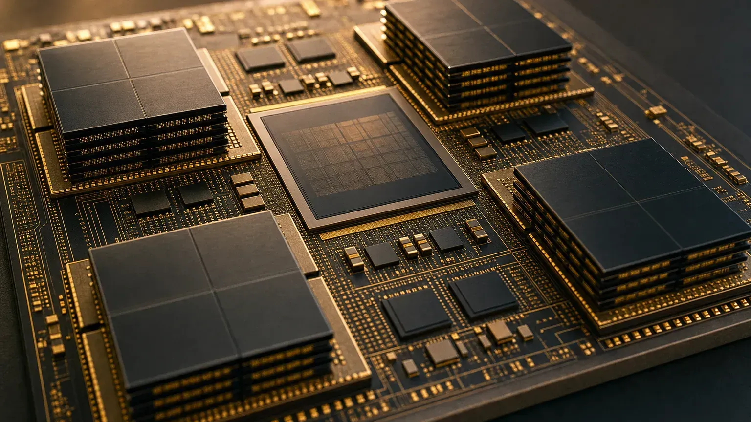
The earlier CoWoS gate covered how TSMC binds a GPU and HBM into one giant module. But CoWoS is only one member of the broad family called “advanced packaging.” As transistors get harder to shrink any further, the industry has shifted the battlefield for better performance outward — from “the chip itself” to “how you assemble chips together.”
This piece spells advanced packaging out. First what it is and why AI needs it, then a breakdown of the 2.5D, 3D, and panel-level routes, and finally a look at Taiwan’s packaging-and-test supply chain, where names like ASE, Unimicron, and KYEC each take their place. This is the deep-dive offshoot of Gate 3, “advanced packaging,” in The AI Hardware Supply Chain, End to End.
What Is Advanced Packaging?
Packaging is the “back-end” step that comes after a chip is finished. Traditional packaging has a simple job: wrap a fabricated chip, hook up the external pins, protect it from damage, and mount it on a circuit board.
Advanced packaging takes a big leap forward. It doesn’t just wrap one chip — it tightly integrates several chips, say a compute chip plus several HBM memory stacks, into a single module using a silicon interposer (a slice of silicon etched with ultra-fine wiring that serves purely as a bridge between chips), a redistribution layer (which reroutes the contacts to positions suited to the package), or direct vertical stacking. The goal is to put the chips close enough together, with short enough wiring, to hit bandwidth that a traditional circuit board could never achieve.
An analogy: traditional packaging is like slipping a book into a jacket to protect it; advanced packaging is like taking several books, notes, and sticky tabs and stacking them precisely the way that’s most convenient for you, then binding them into one reference volume — so you barely waste a moment flipping between them.
Why AI Needs Advanced Packaging
For decades, chips got stronger through process scaling: making transistors ever smaller so more would fit in the same area. But once you get to 3nm and 2nm, the cost and difficulty of shrinking one more step rise sharply while the performance gains grow ever more limited.
So the industry opened a second route: assembling multiple “just-right” chips together in a smarter way, where the overall performance and cost work out better. That route is advanced packaging. It matters especially for AI chips, because a high-end GPU has to pack a compute core together with several HBM stacks and push tens of terabytes of data per second — something simply impossible without advanced packaging. That’s why capacity in this stage has become one of the key bottlenecks for how much high-end AI silicon can ship.
Core-Data Snapshot
The numbers below help you grasp the scale and timing of advanced packaging. Figures like capacity and market size are mostly research-firm estimates, so read them for order of magnitude and trend rather than fixating on the decimals.
| Topic | Data | Timing / Nature |
|---|---|---|
| Advanced-packaging market size | About $46B in 2024 (up roughly 19% year on year), heading toward roughly $79.4B by 2030 | Yole 2025 estimate, CAGR about 9.5% (scope includes 2.5D / 3D / fan-out) |
| TSMC 2026 capital expenditure | About $52–56B, of which advanced packaging, testing, and photomasks together account for roughly 10–20% | TSMC official guidance (Q1 2026 call cited the high end of the range) |
| TSMC CoWoS monthly capacity | About 110k–140k wafers/month by end-2026 (heading toward roughly 170k in 2027) | Analyst / research estimate, not TSMC official |
| SoIC (3D stacking) | 3nm SoIC entered volume production in 2025 | TSMC 2025 Annual Report |
| ASE panel-level packaging line | 310mm×310mm, volume production expected in 1H 2027 | ASE announcement, May 2026 |
The Advanced-Packaging Family Tree: 2.5D, 3D, and Panel-Level
Advanced packaging is a whole family of technologies, most often grouped into three big categories.
2.5D: lay chips side by side on the same base. The marquee example is TSMC’s CoWoS, which places a compute chip and several HBM stacks on a single silicon interposer (a slice of silicon etched with ultra-fine wiring that serves purely as a “bridge”), packed tightly together. Another is InFO, a fan-out type of packaging that uses a redistribution layer to replace part of the interposer; it’s common in mobile chips and some networking chips.
3D: stack chips directly on top of one another. The marquee example is TSMC’s SoIC, which bonds chips vertically with ultra-fine contacts, giving higher density and shorter signal distances than 2.5D. TSMC’s 3nm SoIC already entered volume production in 2025. In practice 3D and 2.5D can be combined: first use SoIC to stack a few small chips into one block, then drop the whole thing into a CoWoS module.
Panel-level packaging (FOPLP): swap the round wafer for a large square panel. Wafer-level packaging mostly uses round wafers as the carrier, which wastes the corners; panel-level packaging switches to a large square panel, with better area utilization, a shot at lower unit cost, and suitability for larger packages. ASE unveiled a 310mm×310mm panel-level packaging line in May 2026, with volume production expected in 1H 2027; TSMC is also building a related pilot line (CoPoS). The industry broadly expects this route to ramp gradually only around 2027 to 2029.
How CoWoS and SoIC Differ
These two names get mixed up most often, but the difference is intuitive: the direction is different.
CoWoS is “horizontal.” It lays chips and HBM side by side on a silicon interposer, like setting several Lego blocks tightly together on the same baseplate. SoIC is “vertical.” It stacks chips on top of one another, bonded directly with contacts far finer than a hair, like stacking Lego layer upon layer. The upside of vertical stacking is shorter distances and higher density, but the process is harder and yield is tougher to hold.
The key point to remember is that they can be used together. For instance, some high-end designs first use SoIC to stack a few small chips, then drop them into a CoWoS module to integrate with HBM.
Taiwan’s Packaging-and-Test Supply Chain: Who Does What
The industry roles in advanced packaging are more finely divided than you might think, and Taiwan has a complete supply chain across several of those links. Laying the names out and sorting them by role is more useful than rote-memorizing company names.
The foundry’s advanced packaging: TSMC. The most cutting-edge CoWoS and SoIC are mainly in TSMC’s hands. On its Q1 2026 call, TSMC acknowledged that advanced-packaging capacity remains tight and that it has to share the load with packaging-and-test partners (OSATs), but it has not disclosed exactly which processes or which customers it outsources.
Packaging-and-test contractors (OSAT): ASE Technology Holding, Amkor, Powertech. These firms handle contract assembly and testing. ASE Technology Holding (including subsidiary SPIL) is the leader in integrated packaging-and-test services, and its own VIPack platform covers fan-out, 2.5D/3D, and other advanced-packaging types; Amkor of the US is also expanding an advanced-packaging plant in Arizona; and Powertech, beyond memory and logic packaging-and-test, is developing panel-level fan-out. When AMD announced its Taiwan investments in May 2026, it named ASE, SPIL, and Powertech among the partners co-developing new packaging.
Test-focused: KYEC. It’s worth being clear here: KYEC’s core is “testing” (wafer probing, final test, burn-in, and so on), not being the main body of advanced-packaging assembly. Within the chain it ensures chip yield, a role distinct from packaging contractors.
Back-end work such as driver ICs: Chipbond. Chipbond’s focus is on driver ICs and display-related back-end packaging-and-test (bumping, COG/COF, and so on), a different field from the advanced packaging of AI compute chips.
IC substrates: Unimicron, NanYa PCB, Kinsus. Here it helps to clarify the difference between “substrate” and “packaging.” A substrate is the key material inside a package that carries the chip and makes the electrical connections (high-end ones use ABF substrates); Unimicron, NanYa PCB, and Kinsus are important suppliers, but what they supply is material, not contract packaging. AMD’s Taiwan investment announcement also separately named all three for their substrate technology.
Equipment side: Scientech, Grand Process Technology, GPM, ASE-affiliated equipment names, and others. These firms supply equipment and process steps such as wet processes, temporary bonding, and die sorting and die bonding. They each have entry points across CoWoS, SoIC, and panel-level packaging, but which customers they actually map to and how much of revenue that represents is limited in public disclosure, and the pairings the market cites are mostly analyst speculation.
How to Read “Advanced-Packaging Concept Stocks”
“Advanced-packaging concept stocks” are a common supply-chain theme in Taiwan’s stock market. The market usually lumps the entire supply chain — packaging-and-test, substrates, equipment, materials — into this group for discussion.
Understanding these companies’ roles in the supply chain is genuinely helpful for grasping the industry’s division of labor. But two things need to be clear up front. First, these companies’ actual customers and orders are mostly kept confidential, so when the market maps them to a given AI-chip heavyweight, that’s often analyst speculation or market chatter, not a company announcement — being listed doesn’t mean orders are already won or benefits guaranteed. Second, the heat of a theme and an individual company’s operations are two different things. This article only describes industry roles and the supply chain’s division of labor; it does not compile beneficiary stocks, nor does it constitute investment advice.
Reading it as a map of “who’s on this chain and what role they play” is far more practical than using it as a stock-picking list.
Key Takeaways for This Gate
After looking at advanced packaging, first remember its positioning: as process scaling gets ever more expensive, precisely assembling multiple chips together has become another route to better performance.
It spans 2.5D (CoWoS, InFO), 3D (SoIC), and panel-level packaging, among other routes. TSMC holds the most cutting-edge CoWoS and SoIC, with 3nm SoIC in volume production since 2025; CoWoS capacity is still supply-constrained, and TSMC will expand it together with packaging-and-test partners, but the outsourcing details and customer specifics have not been disclosed. Taiwan has a complete supply chain across packaging-and-test, substrates, and equipment, with finely divided roles — but understanding roles and picking stocks are two different things.
To see how CoWoS binds up GPU shipments, go back and read What Is CoWoS; to see packaging’s next material trend, see glass substrates; to see Taiwan’s whole semiconductor division of labor, see Taiwan’s semiconductor supply chain; to revisit all eight gates of the chain, head back to the supply-chain overview.