Every time an AI headline says “TSMC’s CoWoS capacity is sold out again,” most people only catch the part about shortages. Few can say what CoWoS actually is, and even fewer see why a packaging technology can dictate the shipping pace of the entire AI-chip industry.
This piece lays it all out at once. First we’ll nail down what CoWoS is and how it relates to “advanced packaging,” then why it becomes the chokepoint for the whole chain, and finally why Taiwan happens to sit right in the center. This is the deep-dive version of Gate 3 in The AI Hardware Supply Chain, End to End.
What Is CoWoS? One Sentence and One Analogy
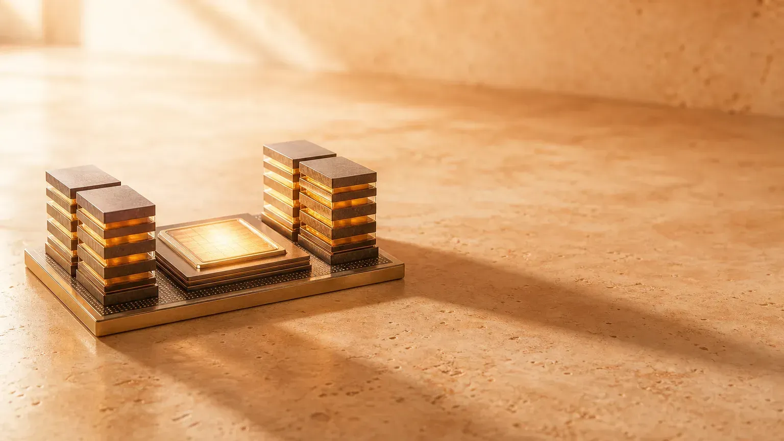
CoWoS stands for Chip on Wafer on Substrate, a TSMC 2.5D advanced-packaging technology. What it does is actually pretty simple: it takes a GPU die and several HBM high-bandwidth memory stacks, places them on the same “interposer” pressed tightly together, then fixes that onto a substrate to form one oversized AI accelerator module.
Here’s an analogy. Traditional packaging is like building the compute chip and the memory separately, then connecting them with traces on a circuit board — leaving a fairly long path between the two. CoWoS is more like gluing several Lego pieces precisely onto the same baseplate to make one “big brick,” bringing the die and the memory close enough to almost touch.
Why go to all this trouble? Because the data a new-generation GPU and its HBM need to move every second runs from a few terabytes up to the twenty-some terabytes of the next-gen Rubin. Stretch the distance and the signal weakens, latency rises, and the whole chip slows down. Traces on a traditional circuit board simply can’t reach that level — the only fix is packaging that presses the chips extremely close. Remember it in one line: CoWoS is the technology that lets a GPU and its memory work face-to-face.
What Is Advanced Packaging, and How Does It Relate to CoWoS?
Many people treat “advanced packaging” and “CoWoS” as synonyms. In fact, the former is the broad category and the latter is one of its signature techniques.
The old packaging logic was “one chip, one package,” relying on the motherboard to connect the processor and the memory. Advanced packaging changes that game, broadly along two routes: one places multiple chips side by side on a silicon interposer to shorten the traces between them — this is often classified as 2.5D; the other simply stacks chips vertically into a 3D IC, using through-silicon vias to connect top and bottom.
Within this family, TSMC has a full set of brands: CoWoS is 2.5D, pressing a GPU and HBM side by side; SoIC goes 3D stacking; and InFO is a thinner fan-out package common in phone chips. CoWoS gets named most often because it lines up precisely with this wave of AI accelerators’ most urgent need.
CoWoS itself comes in three flavors, differing in what “that board in the middle” is made of: the earliest CoWoS-S uses a single silicon interposer with the highest density; CoWoS-R switches to a resin-based redistribution layer for more flexibility; and CoWoS-L uses “local silicon bridges” to link multiple dies, enabling larger packages that fit more HBM — exactly the version today’s top-end GPUs use, and the one in shortest supply.
For readers, one hierarchy is enough to remember: advanced packaging is the category, and CoWoS is the variant tailor-made for AI GPUs within it.
Core-Data Snapshot
The table below is key to understanding the CoWoS shortage. To be clear up front, this capacity is mostly estimates from research firms or industry media, not TSMC’s official month-by-month figures, so focus on the “growth slope” rather than any precise number.
| Time | TSMC CoWoS monthly capacity (wafers/month) | Nature |
|---|---|---|
| End of 2023 | About 14,000-15,000 | Estimate |
| End of 2024 | About 30,000+ (close to 40,000 including outsourced assembly/test) | Estimate |
| End of 2025 | About 70,000-80,000 | Estimate |
| End of 2026 (target) | About 120,000-130,000 (conservative range ~115,000-130,000) | Target / industry estimate |
In just three years, monthly capacity has charged from a little over ten thousand to more than 120,000 wafers — an eight- to nine-fold expansion. Even so, capacity is still being chased by demand, which brings up the next question.
Why CoWoS Becomes the Chokepoint for the Whole AI Supply Chain
The logic isn’t complicated: almost no high-end AI accelerator skips CoWoS or similar 2.5D packaging. Nvidia’s B200, B300, GB300, the next-gen Rubin platform, and even AI ASICs like Google’s in-house TPU — these chips, often tied to several HBM stacks, nearly all have to pass through this gate. So CoWoS monthly capacity becomes one of the most critical bottlenecks for high-end GPU shipments.
One fair caveat: CoWoS isn’t the only gate. Advanced process nodes, HBM, and substrates can all jam up too. It’s just that packaging is especially tight. On its Q1 2026 earnings call, TSMC acknowledged that advanced-packaging capacity is strained and that it has to expand alongside outside assembly-and-test houses to keep up; research firms generally believe this 2.5D-packaging shortage won’t ease somewhat until 2027. In other words, even if the wafers can be made and HBM can be supplied, as long as CoWoS can’t be slotted into the line, the whole AI accelerator still can’t ship.
There’s an easily overlooked takeaway here: in this round of the AI race, “who can secure CoWoS capacity” sometimes decides shipment volume earlier than “whose chip design is stronger.” Watching the supply-chain bottleneck often reveals which way the wind is blowing earlier than watching product launches does.
Who Can Make It? The Division of Labor Between TSMC and the Test Houses
The dominant player at this gate is TSMC, but it doesn’t carry the load alone.
TSMC keeps building dedicated advanced-packaging fabs and holds the highest-end, most complex CoWoS-L in-house. When demand is simply too full, it outsources the relatively standard parts to specialized assembly-and-test houses (the industry calls them OSATs), with ASE Technology Holding and Amkor often named. The industry estimates that CoWoS-class capacity at firms like ASE will expand to roughly 20,000-25,000 wafers a month in 2026 — equally striking growth.
But by sheer volume, these test houses currently look more like a “safety valve,” absorbing TSMC’s overflow orders rather than standing as a co-equal second source. To be clear, what they take on is mostly the relatively standard parts or partial steps, not a full clone of TSMC’s highest-end CoWoS-L. And ASE’s SPIL unit is itself a Taiwanese company, so even when orders are outsourced, most links stay within Taiwan’s supply chain. For readers curious about “advanced packaging stocks,” this division-of-labor line is a starting point for understanding who gets which slice — but how much each company can take on, and at what margin, still comes back to their financial statements, and this article makes no investment judgment.
Why Taiwan Sits at the Center of This Chain
The bulk of CoWoS capacity is highly concentrated in a handful of fabs in Taiwan’s science parks, and most new expansion projects land in Taiwan too. That means at the layer of “2.5D packaging of GPU plus HBM,” Taiwan is one of the single most critical geographic concentration points in the world.
Connecting this with the previous gate makes it clearer: a high-end AI chip first has to be etched by TSMC’s advanced process, then sealed up by TSMC’s CoWoS — the two tightest links both rest on the same island. If supply from Taiwan were cut off, companies like Nvidia and Google would, in the short term, find almost no equivalent replacement capacity for their high-end AI platforms. That’s why this single point draws such close attention from the global tech and capital markets: it directly drives the supply of the world’s AI compute.
What to Watch Next: CoWoS-L, Glass Substrates, and Panel-Level Packaging
This gate is still evolving fast, with three technology directions worth tracking over the long run.
First, CoWoS itself keeps scaling up. At its 2026 technology forum, TSMC revealed it can now build CoWoS at 5.5x reticle (reticle being the largest area a single exposure can produce), with plans for a 14x reticle version in 2028 — at which point one package could integrate roughly 10 compute dies and 20 HBM stacks. Packages keep getting bigger precisely to feed next-gen GPUs that crave ever more data.
Second is the glass substrate, which replaces the traditional organic substrate with glass and could in theory support larger, flatter packages. But to be clear: it isn’t a CoWoS replacement in 2026. Intel showed samples in early 2026, but most players’ mass-production timelines fall in 2027 to 2028.
Third is panel-level packaging (TSMC calls it CoPoS), moving packaging from round wafers onto larger rectangular panels to process more units at once and push costs down. TSMC is already building a pilot line, but mass production is generally pegged at 2028 to 2029.
None of these can replace CoWoS in the short term; they’re more like a relief squad that “extends its life” and “upgrades” it. Whoever first gets them to mass-production yield will pull the next round of advanced-packaging clout in their direction.
Key Takeaways
After this gate, a few things are worth remembering.
CoWoS, stripped down, is the advanced packaging that lets a GPU and HBM work face-to-face, and almost no high-end AI chip can get around it. Its monthly capacity roughly frames the ceiling for high-end GPU shipments; supply clearly fell short of demand in 2025 to 2026, to the point that even TSMC had to bring in test houses as a safety valve.
More important is location. The bulk of CoWoS capacity is concentrated in Taiwan and, together with the advanced process, forms one of the most sensitive single points in the global AI supply chain. That is both Taiwan’s strategic value and the risk the rest of the world watches most closely.
To read on about HBM high-bandwidth memory — which feeds data to the chip and is just as tight — head back to The AI Hardware Supply Chain, End to End; to see how all eight gates of the chain string together, see the supply-chain overview.