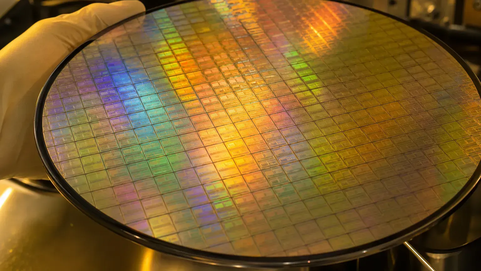
NVIDIA designs the most sought-after AI chips on the planet, yet it doesn’t own a single fab. Apple and Qualcomm are the same — they only draw the blueprints and don’t manufacture anything themselves. So who actually makes these chips? Most of the time, the answer is the same name: TSMC.
This piece spells out the foundry business. First what it is and how it differs from the traditional IDM, then why the foundry model works, who’s in it, what a leading-edge process is, and why nearly all of the most advanced AI chips are made in Taiwan. This is the beginner’s edition of Gate 4, “Foundry,” in The AI Hardware Supply Chain, End to End.
What Is a Foundry?
A foundry is a business dedicated to “making chips for other people.”
The modern chip industry runs on a division of labor: many companies only “design” chips and don’t build their own fabs. These are called fabless companies (fabless semiconductor companies), and NVIDIA, Apple, and Qualcomm are all examples. They hand their blueprints to a foundry to produce. The foundry, in turn, focuses entirely on manufacturing — it doesn’t design and doesn’t sell chips under its own brand.
Here’s an analogy: a fabless company is like a celebrity chef who designs the menu, while a foundry is like a giant central kitchen that cooks each chef’s recipe to order without opening a restaurant of its own to compete. TSMC is the largest such central kitchen in the world.
Core-Data Snapshot
The numbers below help you grasp the scale of this gate. Most market shares are research-firm estimates, so read them for orders of magnitude and trends.
| Topic | Data | Timing / Nature |
|---|---|---|
| TSMC global foundry market share | About 70% (by revenue) | TrendForce, Q4 2025 estimate |
| Ranks two through five | Samsung about 7%, SMIC about 5%, UMC about 4%, GlobalFoundries about 4% | Same as above |
| TSMC leading-edge share | Nodes below 7nm account for about 74% of its wafer revenue | TSMC official, Q1 2026 (own figures) |
| TSMC 2026 capex | About $52–56 billion (toward the high end of guidance) | TSMC official, Q1 2026 earnings call |
| Taiwan’s share of the most advanced semiconductors | Estimated over 90% | CSIS, as of 2023 (advanced-semiconductor basis) |
The Foundry Model: Splitting Design from Manufacturing
To understand the foundry, you first have to understand how it differs from the old model.
In the early days, most major chip companies were IDMs (integrated device manufacturers), handling design, manufacturing, and sales all under one roof, with Intel as the standard-bearer. The problem is that building a leading-edge fab routinely costs tens of billions of dollars — not every design company can afford that. In 1987, TSMC pioneered the “pure-play foundry” model: it only manufactures, doesn’t design, and doesn’t sell own-brand chips, which means it never competes with its customers.
That “we don’t compete with our customers” positioning is the key. It lets companies like NVIDIA and Apple safely hand their most confidential designs to TSMC, and it lets design firms focus on innovation while the foundry focuses on pushing yield and capacity to the limit. As a result, the whole industry divides labor more finely and moves faster.
Who’s in the Foundry Business
Lay out the main players and you’ll see this gate is highly concentrated.
TSMC holds the largest share — roughly 70% globally in Q4 2025 — with leading-edge processes heavily concentrated there. Samsung ranks second, running a foundry alongside its own design division, for a single-digit share. SMIC sits around third, focused on mature nodes. UMC and GlobalFoundries focus on mature and specialty nodes, each holding around 4%. Intel has also restarted its foundry business in recent years (Intel Foundry), but external-customer revenue is still small and it’s still in catch-up mode.
One common misconception to clear up: market-share numbers vary a lot depending on whether you “count the in-house design division” and whether you measure by “revenue or by capacity.” Here we use research firms’ pure-play foundry revenue basis, describing the industry landscape — not rating any individual stock.
Leading-Edge vs. Mature Process
A foundry’s “process node” gets compared constantly, so let’s grab the big-picture concept first.
A process node (such as 5nm, 3nm, or 2nm) can be loosely understood as a technology generation; the smaller the number, the more transistors usually fit into the same area and the lower the power — but R&D and manufacturing also get more expensive and harder. The industry commonly calls nodes below 7nm leading-edge, and high-end AI chips almost all use this tier; by TSMC’s own wafer revenue, nodes below 7nm contribute about 74%.
But don’t forget that mature nodes at 28nm and above carry just as much demand — automotive chips, display drivers, and power management all rely on them. Whether a process is the right fit depends on where it’s used; more advanced isn’t always more suitable. For a deeper dive into 2nm, GAA, and other leading-edge details, see the leading-edge process gate; to learn about the manufacturing equipment, see ASML and lithography equipment.
Why It’s Concentrated in Taiwan, and How It’s Diversifying
The most advanced foundry capacity is heavily concentrated in Taiwan, and that’s no accident.
Research estimates that Taiwan produces more than 90% of the world’s most advanced semiconductors. The concentration has three layers: first, the customers and technology TSMC has accumulated through its pure-play model; second, the fact that volume production of new nodes demands R&D, equipment, materials, and talent in close proximity, so TSMC’s most advanced processes (such as 2nm) are deployed in Taiwan first; and third, the complete supply chain and clustered fab campuses Taiwan has already built up.
In recent years, to spread risk and stay close to customers, TSMC has also expanded its fabs overseas: in Arizona it plans to invest $165 billion to build several fabs and advanced-packaging facilities (including more advanced nodes), while Kumamoto in Japan and Dresden in Germany lean toward automotive, mature, and specialty processes. But the most cutting-edge production core still stays in Taiwan. This “concentrated in Taiwan” reality is precisely the root of the supply-chain-concentration risk discussed across the whole supply chain.
Key Takeaways for This Gate
After looking at the foundry, first remember its essence: it splits the chip industry into design and manufacturing. Fabless companies focus on design, foundries focus on manufacturing, and that division of labor makes the whole industry run faster.
TSMC stays firmly at number one thanks to its pure-play model, leading-edge processes and packaging, and cluster effects — roughly 70% in Q4 2025, with nearly all of the most advanced AI chips depending on it for production. That also makes Taiwan the most pivotal, and most closely watched, link in the global AI supply chain.
To dig into process nodes and 2nm details, see the leading-edge process; to see the lifeline of manufacturing equipment, see ASML; to see Taiwan’s entire semiconductor division of labor, see Taiwan’s semiconductor supply chain; to step back and view all eight gates of the chain, return to the supply-chain overview.