The earlier ASML gate covered ASML the company; this piece focuses on the technology that lets it stand alone in the world: EUV. It’s the key piece of equipment you can’t get around when making the most advanced chips.
This piece spells EUV out plainly. First what it is and why advanced processes need it, then how it works, why only ASML can build it, who uses it, and why it became the core of export controls. This is the technical deep dive of the ASML/EUV gate within The AI Hardware Supply Chain, End to End.
What EUV Is
EUV’s full name is Extreme Ultraviolet Lithography. Its core is a single number: a wavelength of just 13.5 nanometers.
Lithography is the step that “prints” a circuit pattern onto a wafer, and the shorter the wavelength of the light used, the finer the lines you can draw. The previous mainstay, DUV (deep ultraviolet), used 193 nanometers; EUV shrinks the wavelength all the way down to 13.5 nanometers, the equivalent of switching to a far finer light-pen. By way of analogy: DUV is like tracing over lines repeatedly with a thicker pen to bring out the detail, while EUV can print the most critical fine features in just a few passes.
One common misconception is worth clearing up first: EUV is mainly used on the most complex critical layers. Without it, some nodes can still be forced through with DUV multi-patterning, just at heavy cost, cycle-time, and yield pressure. Below 7nm, EUV prints these critical layers finer and with less effort in a single pass, which is why advanced processes that want to be competitive on cost and efficiency almost all rely on it.
The Principle: Light Made From Tin Droplets
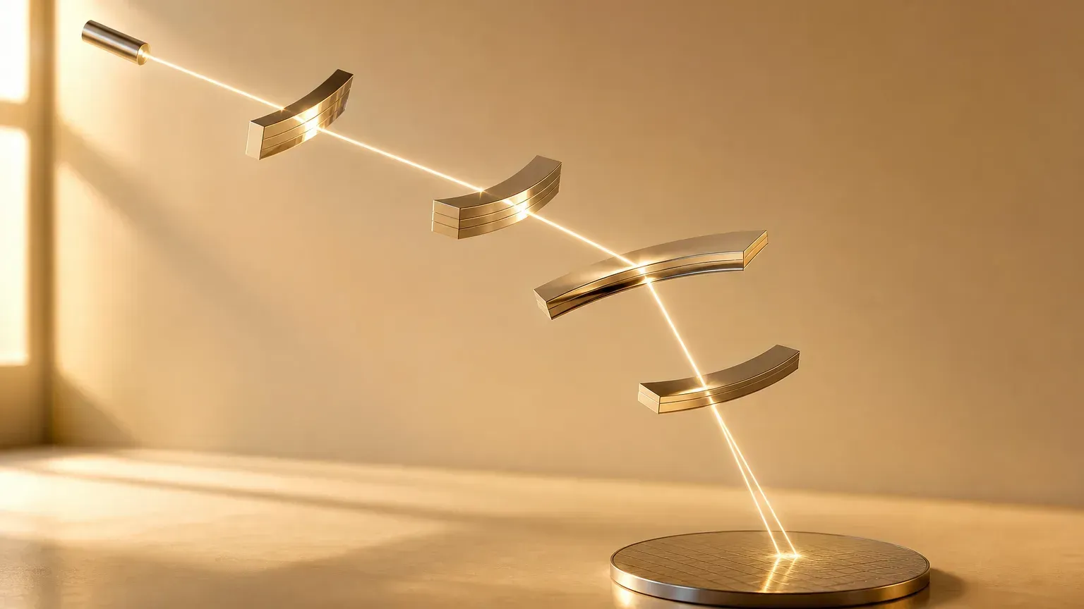
EUV light isn’t something an ordinary bulb can produce, and the process to generate it is fairly violent. ASML’s approach is this: shoot out molten tin droplets about 25 microns in diameter at high speed, first flatten them with a low-energy laser, then hit them with a high-energy laser to turn them into plasma, which momentarily emits EUV light — and this action repeats about fifty thousand times a second.
What makes it even trickier is that EUV is absorbed by almost everything, including air, so the entire light path has to run in a high vacuum. It also can’t be refracted with lenses the way visible light can, and can only be reflected and focused by layer upon layer of precision multilayer mirrors. Behind this, beyond ASML’s own decades of accumulated work, lies top-tier optics supplied by Germany’s ZEISS. Add it all up and you can see why only ASML in the world can build it.
Low-NA and High-NA, Plus the Price
EUV machines come in two generations.
Low-NA EUV (the NXE series, numerical aperture NA 0.33, resolution around 13 nanometers) is the current mass-production workhorse, carrying the advanced processes from 7nm and 5nm to 3nm and even 2nm. High-NA EUV (the EXE series, NA 0.55, resolution around 8 nanometers) is the more advanced next generation, able to print finer and aimed at nodes beyond 2nm; in 2026 it just crossed the technical threshold that lets customers bring it into mass production, but actually integrating it into production lines is estimated to take another two to three years, with the first chips exposed using it expected to start appearing within a few months.
On price, ASML doesn’t publish per-unit figures, but estimating from public reporting and financial filings: Low-NA runs on the order of $200 million, while High-NA is on the order of $350 million to $400 million, roughly double the former. A single machine weighs hundreds of tons and takes multiple cargo planes to ship, making it one of the single most expensive pieces of equipment in the semiconductor industry.
Who Uses It, and Export Controls
All three of the big advanced-process makers rely on EUV. TSMC was the world’s first to bring EUV into mass production, with its N7+ process back in 2019, then used it heavily on N5 and N3, and put 2nm (N2) into mass production in 2025; for now TSMC is still choosing to extend Low-NA EUV and has not announced plans to adopt High-NA. Samsung has used EUV since 7LPP, bringing it even into memory (DRAM). Intel began EUV mass production with Intel 4 and has already placed High-NA machines in its R&D line in Oregon, USA, aiming at more advanced nodes like 14A.
The other side is export controls. ASML’s most advanced EUV machines are subject to Dutch and U.S. controls and have never been sold to Chinese customers. Because the critical layers of advanced processes depend heavily on EUV, and EUV comes from ASML alone and is under controls, it has become a key node in the U.S.-China chip rivalry, and is one of the cores of both The Chip War and Export Controls. This article only states the facts of the controls and makes no political judgment.
The Supply Chain and Taiwan’s Role
EUV’s core system is integrated by ASML, its light-source technology traces back to Cymer (which ASML acquired), and the most critical optics (lenses and mirrors) are supplied exclusively by Germany’s ZEISS. These two are the hardest parts of EUV to replicate.
Taiwan’s firms participate mostly on the periphery. Gudeng Precision makes the EUV reticle POD (reticle transport box) and is one of the few Taiwanese firms certified by ASML, a relatively well-defined role; TSMC itself has world-class mask-making and pellicle (mask-protection film) capabilities. Other mask, materials, carrier, and engineering-service firms the market mentions are mostly supply-chain speculation by industry media and analysts. To be especially clear: these lists represent “possible roles,” not that anyone has already won orders from ASML or TSMC, nor how much they stand to benefit. This article only describes industry roles; it does not compile beneficiary stocks, does not rank individual stocks, and does not constitute investment advice.
Why It Has the Lifeblood in a Chokehold
The reason EUV is the lifeblood comes down to three things stacking together.
It satisfies three conditions at once: the hardest few layers of advanced processes need it, only ASML in the world can build it, and export controls cut some countries out of it. Any one of these is critical on its own; stacked together, EUV goes from a piece of equipment to the geopolitical gate to “advanced-process capacity.” Who can use it, how many units, and which generation, to a degree, decides who can make the most advanced chips.
Key Takeaways for This Gate
EUV is extreme-ultraviolet lithography, using light at a 13.5-nanometer wavelength to print the finest circuits, and it’s the workhorse for the most critical few layers of advanced processes. It’s generated from tin-droplet plasma, needs to be focused with mirrors in a vacuum, and only ASML in the world can mass-produce it; it comes in Low-NA and the more advanced High-NA, with a single machine costing roughly $200 million to $400 million.
TSMC, Samsung, and Intel all rely on it to make their most advanced chips; and because it comes from a single firm and is under export controls, it has become a key node in the chip war. Taiwan’s firms participate mostly on the periphery, in areas like reticle PODs, masks, and materials, and the related lists are mostly analyst speculation, so just understanding the roles is enough.
To read about ASML the company, go back to What Is ASML; to see how the chips EUV prints get manufactured, read Foundry and Advanced Process; to see the controls and geopolitics, read The Chip War; to look back at the whole chain, head back to the supply-chain overview.