For every generation of AI chips to get stronger, memory has to feed them faster. While NVIDIA’s Blackwell is still using HBM3e, the next generation — HBM4 — is already in mass production and on the field. So what exactly did it upgrade, and why is it the key to the next generation of AI chips?
This piece spells out HBM4. First how it differs from HBM3e and why doubling the interface is the point, then the base-die change, the progress at the three makers, and why NVIDIA’s next-gen Rubin is specified to use it. This is the generational-spec offshoot of the HBM gate.
What Is HBM4?
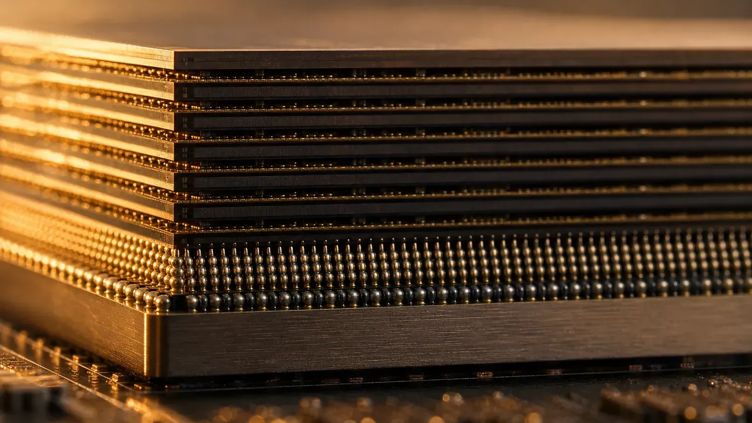
A quick refresher first: HBM (high-bandwidth memory) stacks multiple DRAM dies vertically and connects them to the GPU through an ultra-wide interface, so the chip doesn’t starve waiting for data. HBM3e is the version the current Blackwell generation uses; HBM4 is the next generation.
This generation, HBM4 changes the structure — it doesn’t just push the old version’s speed higher. The two most critical changes: one is widening the external interface from 1024-bit to 2048-bit, effectively doubling the data channel; the other is switching the base die at the bottom — the one that handles communication — to a logic process. These two changes let HBM4 jump a level in both bandwidth and power efficiency.
Core-Data Snapshot
Below we capture the order of magnitude of HBM4’s specs. Keep the two yardsticks straight: the “JEDEC standard” versus “each maker’s beyond-spec products.”
| Topic | Data | Timing / Nature |
|---|---|---|
| External interface | HBM3e is 1024-bit; HBM4 is 2048-bit | JEDEC standard |
| Per-stack bandwidth (standard) | HBM4 up to about 2 TB/s | JEDEC standard ceiling |
| Per-stack bandwidth (products) | Samsung claims up to 3.3 TB/s; Micron claims >2.8 TB/s | 2026, each maker’s product spec |
| Capacity | Supports 4/8/12/16-layer stacks, up to 64GB per stack | JEDEC standard |
| base die | Switches to a logic (foundry) process (e.g. Samsung 4nm, TSMC advanced logic) | 2025-2026, official |
HBM3e to HBM4: What Changed
Put the two generations side by side and the differences are clear.
Interface width doubles: this is the most central upgrade. HBM3e is 1024-bit; HBM4 widens to 2048-bit. Think of it as widening a highway from “1024 lanes” to “2048 lanes” — at the same speed, the traffic that can pass through roughly doubles.
A big leap in bandwidth: mainstream HBM3e products run at about 1.2TB per second; HBM4’s JEDEC standard is 2TB per second, and the makers’ actual products claim as high as 2.8 to 3.3 TB/s.
Base die switches to a logic process: that base die at the bottom moves from a DRAM process to a logic process — for example Samsung’s 4nm, or an advanced logic process in partnership with TSMC. This lets the bottom chip pack in more control and custom features, so HBM becomes more like a customizable “memory plus logic” platform.
Better power efficiency: SK hynix and Samsung both claim HBM4 improves power efficiency by around 40% versus the prior generation, while Micron claims over 20% for its own 12-layer products.
The Three Makers’ HBM4 Progress
The HBM4 contest is still a battleground for these three: SK hynix, Samsung, and Micron.
Samsung announced HBM4 mass production and commercial shipments in February 2026, with product specs claimed as high as 3.3TB per second. Micron’s 36GB 12-layer HBM4 entered mass production in the first quarter of 2026, explicitly built for NVIDIA’s Vera Rubin platform. SK hynix also completed HBM4 development and established a mass-production system, with published specs of 2048 I/O, over 10Gb per second, and a power-efficiency gain of over 40%.
Worth flagging: who slots into NVIDIA’s next-gen spec first, and whose yield is higher, are the decisive factors in this fight — and those are still in progress. Taiwan’s local firms don’t make the HBM itself; their role is in packaging and test peripherals (for details, see HBM stocks).
Why the Next Generation of AI Chips Can’t Do Without It
HBM4 upgrades this way because it’s being forced to by the appetite of next-gen AI chips.
NVIDIA’s planned Rubin GPU can carry up to 288GB of HBM4 per chip. Inference-style, long-context AI workloads have far more data to move than before, and once memory bandwidth and capacity can’t keep up, even the strongest compute cores can only wait idle. HBM4’s doubled interface and high bandwidth exist precisely to keep the data supply matched to compute at the level of something like Rubin.
In other words, HBM4 is the “conveyor-belt upgrade” for next-gen AI chips. Without it, no matter how high the compute, it gets bottlenecked by memory.
Key Takeaways for This Gate
After looking at HBM4, remember two core upgrades first: the external interface doubles from 1024-bit to 2048-bit, and the base die switches to a logic process. These two points buy a big leap in bandwidth and power efficiency.
HBM4 is a necessary condition for feeding next-gen AI chips like NVIDIA’s Rubin; Samsung and Micron have announced mass production and shipments, and SK hynix has also completed development and established a mass-production system. When reading specs, remember to keep the two yardsticks straight — the “JEDEC standard” versus “each maker’s beyond-spec products” — so the numbers don’t get muddled.
To first understand what HBM is and why it’s in short supply, go back and read the HBM gate; to see the supply chain and how the stocks divide up the work, see HBM stocks; to see the packaging that binds HBM and the GPU together, see CoWoS; to see all eight gates of the chain, head back to the supply-chain overview.