The “AI chip” in the news sometimes means NVIDIA’s GPU, sometimes Google’s TPU, and sometimes some processor inside your phone. So which one is really the AI chip? The answer, it turns out, is: they all are.
This piece spells out the AI chip. First, why it’s a “family” rather than a single kind of chip; then what GPU, ASIC, TPU, NPU, and FPGA each are and how they differ; and finally the difference between training and inference, and between cloud and on-device. This is the beginner’s overview for Gate 1, “AI chips,” in The AI Hardware Supply Chain, End to End.
What Is an AI Chip?
An AI chip (also called an AI accelerator) is the umbrella term for “hardware optimized for AI workloads,” and it covers several kinds of chips.
Why does it need a dedicated chip? Because AI’s computation has a distinctive character: lots of matrix multiplication, tensor math (a tensor can be thought of as an extension of a matrix — the large tables of numbers a model works through), low-precision calculation, and operations that can run all at once. An ordinary CPU isn’t good at this kind of large-scale parallel computing, so the industry built a variety of chips specialized to accelerate this sort of math, collectively called AI chips.
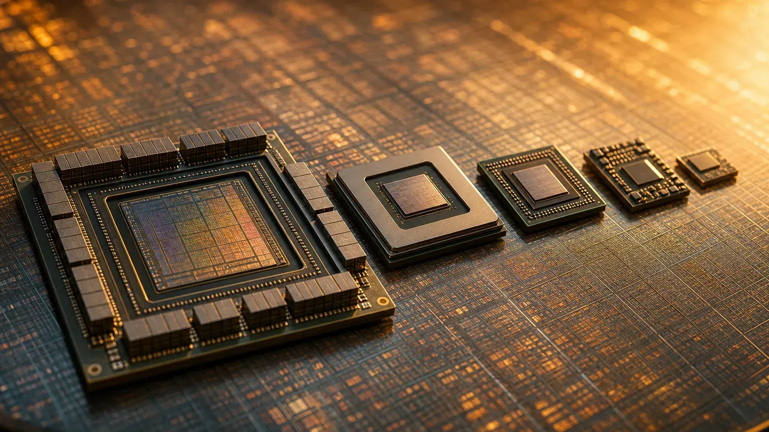
Think of it as a family: GPU, ASIC, TPU, NPU, and FPGA are all members of this family, each with its own specialty, but all born for the same purpose — to run AI’s computation both fast and lean.
Core-Data Snapshot
The few numbers below help you grasp the scale of the AI chip market. Most are research-firm estimates.
| Topic | Data | Timing / Nature |
|---|---|---|
| Global semiconductor revenue | About US$1.32 trillion estimated for 2026 | Gartner forecast |
| AI semiconductor share | About 30% of 2026 semiconductor revenue | Gartner forecast |
| NVIDIA AI chip market share | About 70% | TrendForce, 2025 estimate |
| Cloud in-house ASIC vs GPU growth rate | ASIC about 44.6%, GPU about 16.1% | TrendForce, 2026 estimate |
| AI PC share | Spreading fast; Gartner pushed its 50% penetration point back to 2028 on memory price hikes | Gartner |
The Five AI Chips and What Each Does
Let’s lay the family members out side by side:
| Type | What it is | What it’s good for |
|---|---|---|
| GPU | General-purpose parallel processor, flexible, with a mature ecosystem (CUDA) | Large-model training, cloud inference, research |
| ASIC | Custom chip tailored to a specific task, highly efficient, low on flexibility | Cloud giants’ in-house designs, specific workloads, cost-cutting |
| TPU | Google’s in-house ASIC, specialized for tensor math | Google Cloud, its own models and customer workloads |
| NPU | Low-power AI chip put into phones, laptops, and cars | On-device real-time AI, power-saving, offline-capable |
| FPGA | Reconfigurable (its hardware logic can still be changed after it ships), the compromise between flexibility and efficiency | Low latency, industrial, prototyping |
Want to dig into the GPU? See the GPU gate; want to understand why cloud giants build their own ASICs? See the ASIC gate.
Training Chips vs Inference Chips
Even though both are AI chips, whether one is used for “training” or “inference” changes its priorities a lot.
Training is teaching a model to learn from massive amounts of data, like taking a student from scratch all the way to mastery. It needs enormous compute, very large memory, high-speed chip-to-chip interconnect, and long stretches of stable computation. Inference is the model — once trained and live — quickly giving answers to new inputs, like having the student sit an exam. Inference cares more about latency (how fast it answers), cost, and performance per watt.
The same chip may be able to do both (GPUs and TPUs both can), but because inference keeps generating cost with every single use, the market has more and more “inference-first” chip designs.
Cloud vs On-Device
Where an AI chip sits also determines what it looks like.
Cloud AI chips sit in data centers; their advantage is big compute, scalability, and centralized management, which suits large-model training and high-volume API inference — but they draw a lot of power. On-device AI chips (mostly NPUs) sit in phones, laptops, and cars; their advantage is low latency, privacy protection, offline capability, and bandwidth savings, at the cost of being constrained by size and power. Microsoft’s Copilot+ PC, for instance, requires NPU compute exceeding 40 trillion operations per second.
Put simply: the cloud goes “brute force for the win,” while on-device goes “every bit counts.” More and more AI applications will split the computation — the heavy stuff in the cloud, the real-time stuff on the device.
Key Takeaways for This Gate
After looking at the AI chip, remember the most important idea first: it’s the umbrella name for a “family of accelerators,” not just the GPU.
GPUs are general-purpose with a mature ecosystem; ASICs (including Google’s TPU) are tailored to a specific task and highly efficient; NPUs go low-power and get put into phones and laptops; FPGAs are the compromise between flexibility and efficiency. The 2026 landscape is NVIDIA GPUs still dominating the cloud, while cloud in-house ASICs and on-device NPUs each grow fast. Understand this taxonomy and you’ll see why the AI chips in the cloud, in your phone, and in your car don’t look alike.
Want to dig deeper into the GPU? Read GPU; to see cloud in-house chips, read ASIC; to see the flagship GPU generation, read Blackwell; to step back to all eight gates of the chain, head back to the supply-chain overview.